- »
- Underfill
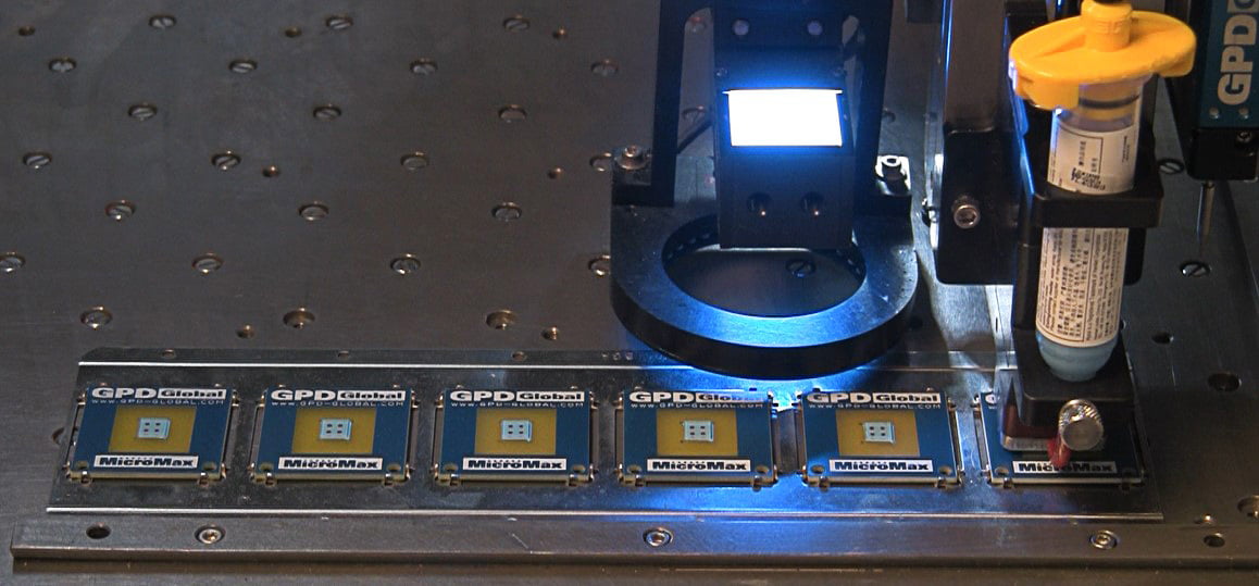
Underfill
What is Underfill?
Underfill is a composite material usually made of an epoxy polymer that fills gaps between a chip and its carrier or a finished package and the PCB substrate to connect the chip to the board.

Types of Underfill Applications
- Ball Grid Array (BGA) Underfill – BGA underfill plays a vital role in electronic packaging, especially for Ball Grid Array (BGA) components. It’s an essential step to ensure the reliability and longevity of these components on circuit boards.
- PCB Underfill – PCB underfill is a vital method that guarantees strong connections and long-lasting performance in contemporary electronic devices.
- Capillary Underfill Dispensing – Capillary underfill involves dispensing a void-free fluid to encase the underside of a silicon die or BGA component. This process enhances connection strength and compensates for thermal expansion differences, ensuring robust and reliable solder joints.
- Flip-chip Underfill – Flip-chip underfill refers to the process of applying a liquid encapsulant, usually epoxy resins with a high concentration of fused silica (SiO₂) particles, between the silicon die (chip) and the substrate after flip-chip interconnection. This step enhances the mechanical strength of solder joints, compensates for thermal expansion differences, and prevents stress concentration in the joints, ensuring the overall reliability of micro-electronic devices.
- Molded Underfill – Molded underfill (MUF) is a process where resin is applied to fill the gaps between the silicon chip (integrated circuit or IC) and the substrate. Unlike traditional methods, where the encapsulation is applied to the side of the chip or package, MUF focuses on filling the gap between the chip and substrate using a single material. Its purpose is to enhance mechanical strength, improve thermal performance, and prevent stress-related issues in electronic packages.
- Board Level Underfill – In the realm of electronic assembly, board-level underfill finds its purpose between completed packages and the printed circuit board (PCB). This technique reinforces mechanical strength, enhances thermal performance, and prevents stress-related issues, ensuring the reliability of modern electronic devices.
- Wafer Level Underfill – Wafer-level underfill entails directly applying an underfill material to the entire wafer before individual chips are separated. This process enhances mechanical strength, improves thermal performance, and prevents stress-related issues in electronic packages.
- Panel Level Underfill – Unlike individual component-level underfill, panel-level underfill treats multiple packages on a single panel as a cohesive unit. Panel-level underfill is employed on large square panels that house thousands of additional packages.
- System-in-Package (SiP) – System in Package (SiP) underfill enhances mechanical strength, improves thermal performance, and prevents stress-related issues in micro-electronic devices. It refers to the process of applying a specially formulated polymeric adhesive to fill the gap between the silicon die (chip/package) and the substrate or printed circuit board (PCB).
- Integrated Passive Device (IPD) – Integrated Passive Device underfill (IPD Underfill) entails using a specially formulated polymeric adhesive to bridge the gap between the silicon die (chip/package) and the substrate or printed circuit board (PCB). Unlike traditional methods, where encapsulation is applied at the component level, IPD underfill treats the entire integrated passive device (including passive components) as a cohesive unit.
- Redistribution Layer (RDL) – Redistribution Layer (RDL) underfill ensures that input/output (I/O) pads are accessible from various locations on the chip, simplifying chip-to-chip bonding.
- Chip-on-Wafer (CoW) – Chip-on-Wafer (CoW) underfill is a crucial method employed in micro-electronic packaging, especially for components like Ball Grid Array (BGA) and Chip Scale Packaging (CSP).
- Chip-on-Wafer-on-Substrate (CoWos) – Chip-on-Wafer (CoW) underfill CoWoS allows for reduced bump heights underneath the chips, important for micro sizing.
- Package-on-Package (PoP) – In Package-on-Package (PoP) underfill configurations, several chips are stacked vertically on top of each other, enabling efficient 3D integration while conserving space.
- Fan-Out Wafer Level Packaging (FOWLP) is a process that packages integrated circuits while they’re still on the wafer, instead of post-dicing. This method enables an increase in the number of contacts without necessitating an enlargement of the die size.
- Organic substrate – Organic substrate underfill, a component used in the encapsulation of integrated circuits, is generally a substance with a high glass transition temperature (Tg) and has a thickness around 100 microns. This underfill enhances the mechanical robustness of the device, aids in the dispersion of thermal stress, and shields the device from harm caused by the environment. It plays a crucial role in fine-pitch bump arrangements, where it is applied prior to the thermocompression bonding procedure.
- Chip Scale Package (CSP) – Chip Scale Package (CSP) underfill, a variety of epoxy substance utilized in the semiconductor sector, is employed to bridge the space between the semiconductor chip and its carrier, or between a completed package and the PCB substrate.
- Edge or corner bond partial underfill – Edge bonding and corner bonding techniques enhance the reliability of electronic devices by strengthening solder joints. While edge bonding fills the gap between components and the PCB, corner bonding reinforces critical areas. On the other hand, partial underfill streamlines the process by selectively applying encapsulant to essential regions, ensuring robust assemblies. These methods collectively contribute to the durability of electronic systems.
- No-flow underfill – No-flow underfill, a category of epoxy substance utilized in the semiconductor sector, is applied to the substrate prior to the positioning of the chip or package. Following this, the chip is situated on the dispensed underfill, leading to a squeeze flow of the material.
Underfill Videos